
Check out the leading manufacturer for a professional coil packing solution here:
A few weeks ago, we had the opportunity to visit a renowned PCB manufacturing company known as PCBWay. In this video, we will delve into the fascinating world of PCB manufacturing, specifically focusing on the board manufacturing process. Join us as we take you on a virtual tour of the PCBWay factory in China and explore how PCBs are made.
PCB manufacturing is an intricate and crucial process in the electronics industry. It involves the creation of printed circuit boards that serve as the foundation for electronic components. These boards provide mechanical support and electrical connections for various electronic devices, making them an essential component in today’s technology-driven world.
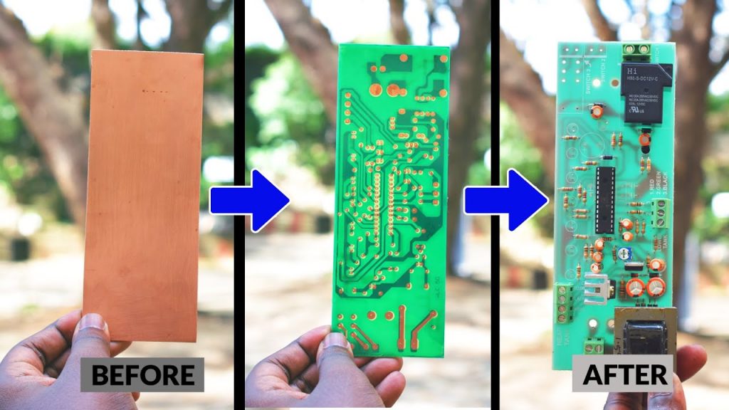
The board manufacturing process begins with the design phase, where engineers create a schematic layout of the circuit. This layout is then converted into a digital file, which is used to fabricate the PCB. The digital file undergoes several steps such as imaging, etching, and drilling to bring the design to life.
Imaging involves transferring the digital file onto a light-sensitive material called the photoresist. This material is then exposed to ultraviolet light, which creates a pattern of the circuit on the board. The unexposed areas of the photoresist are removed, leaving behind the desired circuit pattern.
Next, the board undergoes an etching process, where a chemical solution is used to dissolve the excess copper on the board’s surface. This step ensures that only the copper traces necessary for the circuit remain, eliminating any unwanted conductive paths.
Drilling is the subsequent step, where precision drills create holes in the board to accommodate electronic components and interconnections. These holes are vital for soldering and mounting various components onto the PCB.
Once the drilling is complete, the board goes through a thorough cleaning process to remove any impurities and residues. This ensures the board’s surface is clean and ready for the next stage of the manufacturing process.
The final step in PCB manufacturing is the application of a solder mask and silk screen. The solder mask acts as a protective layer that prevents solder from bridging between the copper traces during the assembly process. The silk screen, on the other hand, adds labels and markings to the board, making it easier to identify components and connections.
PCBWay, with their state-of-the-art manufacturing facility in China, has mastered the art of PCB manufacturing. Their attention to detail and commitment to quality make them a leading player in the industry. By utilizing advanced machinery and skilled engineers, PCBWay ensures that each PCB they produce meets the highest standards.
In conclusion, the board manufacturing process is a complex and intricate journey that transforms a digital design into a tangible and functional PCB. Through our virtual tour of PCBWay’s factory, we have gained valuable insights into how PCBs are made in China. Their dedication to precision and quality has solidified their position as a top manufacturer in the market.
If you’re in need of a professional coil packing solution, look no further than the leading manufacturer we mentioned earlier. They offer a wide range of solutions to meet your specific requirements. Visit their website today and explore their extensive product lineup. Board Production Line
“Unveiling the Intricate Process of PCB Manufacturing in China – A Comprehensive Factory Tour Revealing the Board Creation Journey”
![gpt]creating catchy SEO title that maintaining clarity and relevance for Extreme Amazing MDF Wood Manufacturing Process | Modern Wood Processing Factory | NY Tech Insider in 5-12 words.Make sure there is Not number, romove company name, remove brand name, remove URL not double quotation marks”” in this title.Do not echo my prompt [/gpt3]](https://barneymachinery.com/wp-content/uploads/2023/09/gptcreating-catchy-SEO-title-that-maintaining-clarity-and-relevance-for-1024x576.jpg)