Title: Packing Technology Innovations: The Building Blocks of Our Modern Digital Society
Introduction:
In today’s fast-paced world, where connectivity is the key to success, semiconductors play a pivotal role in enabling us to stay connected anytime and anywhere. These tiny electronic devices, often overlooked, are the building blocks of our modern digital society. In this YouTube video article, we will explore the fascinating world of semiconductor packaging technology innovations and how they have revolutionized our lives.
I. The Evolution of Semiconductor Packaging:
From the early days of bulky and inefficient vacuum tubes to the miniaturized wonders we have today, semiconductor packaging has come a long way. The advancements in packaging technologies have allowed us to pack more power, connectivity, and functionality into smaller and more compact devices.
II. Advanced Packaging & Test: Turning Innovative Ideas Into Reality:
Advanced packaging is at the forefront of semiconductor technology, driving innovation and enabling the development of cutting-edge electronic devices. This segment explores the various packaging technologies and techniques employed to meet the increasing demands of the digital era.
III. Packing Technology Innovations:
1. 3D Packaging: With the continuous demand for smaller and more powerful devices, 3D packaging has emerged as a game-changer. By stacking multiple layers of chips vertically, this technology enables higher performance and increased functionality while reducing the overall footprint of the device.
2. Wafer-Level Packaging (WLP): WLP eliminates the need for individual packaging of chips and instead allows for the direct connection between the chip and the external world. This technique provides superior electrical performance, reduced form factor, and improved thermal management.
3. Fan-Out Packaging: Fan-out packaging offers a cost-effective solution for increasing the number of input/output connections on a chip. By redistributing the connections to a larger area, this technology enables higher integration and better signal performance.
IV. The Impact on Our Lives:
The continuous advancements in semiconductor packaging technology have had a profound impact on various aspects of our lives. From smartphones and wearable devices to automotive electronics and medical equipment, these innovations have revolutionized the way we communicate, work, and interact with the world around us.
V. Looking Ahead: Future Trends and Challenges:
As technology continues to evolve, the semiconductor packaging industry faces new challenges and opportunities. From the rise of Internet of Things (IoT) devices to the demand for enhanced security measures, the future of packaging technology will be driven by the need for increased connectivity, improved performance, and greater energy efficiency.
VI. Conclusion:
Semiconductor packaging technology innovations have played a vital role in shaping our modern digital society. The ability to pack more power, connectivity, and functionality into smaller and more compact devices has revolutionized the way we live, work, and communicate. As we move forward, the industry will continue to push boundaries, meeting the ever-growing demands of our connected world.
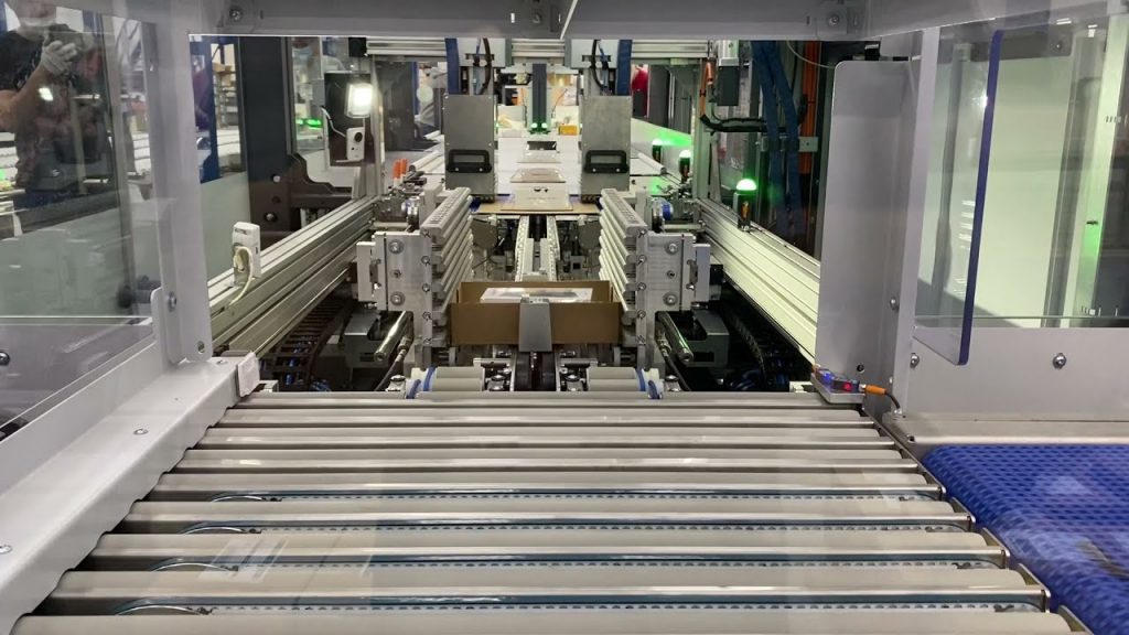
Check the coil packing solution with leading manufacturers for professional solutions just here. Automatic packing line
“Unleashing the Power of Advanced Packaging & Test: Transforming Ideas into Real-World Solutions and Revolutionizing Packing Technology”